
In this post, we’ll explore various techniques and recommendations for creating high-speed printed circuit board designs.
When delving into high-speed designs, two primary areas come into focus. The first is signal integrity (SI), encompassing concerns about crosstalk due to trace spacing, reflections from impedance mismatches, signal attenuation, and issues like ringing. Minimizing these problems is crucial. The second area of focus is electromagnetic interference (EMI).
When does a design qualify as “high-speed,” and when should we start paying attention?
Let’s consider a scenario: imagine we have a 100 MHz clock signal in our design, assuming it’s the highest frequency in our system. However, the challenge isn’t the clock signal’s fundamental frequency but the rise and fall times of this near square-wave clock signal.
These sharp transitions from digital low to digital high (or vice versa) contain much higher frequency content than the fundamental frequency. By considering the signal’s rise and fall times, we can roughly calculate the maximum frequency within the signal (or bandwidth) using a specific formula.
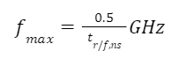
For instance, a 100 MHz clock signal with a 1 ns rise time has a bandwidth of 500 MHz — a significant difference!
When a PCB trace length surpasses 1/12th of the wavelength in the dielectric, a more detailed examination of the PCB design is necessary. This is the point when traces start resembling distributed length transmission lines rather than lumped elements. We term this length the “critical length.”
Pro Tips:
Tip #1: Reference Planes
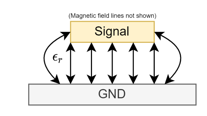
Always ensure a ground or relevant power plane is adjacent to a signal plane, directly below (or above) a layer carrying a trace. This not only maintains proper return paths and minimizes electromagnetic field spread but is also crucial for controlled-impedance traces. For AC signals above a few kHz, the return path lies directly below the signal trace in the reference plane below. A vital rule is to avoid splits in the reference plane beneath traces.
Tip #2: Board Stack-Up
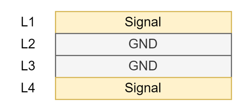
A ground plane should not only be adjacent to a signal plane but also to a power plane. A thin dielectric between planes enhances coupling and allows for thinner traces, providing more space to work with. However, manufacturing thin traces can pose challenges.
Tip #3: Controlled Impedance Traces
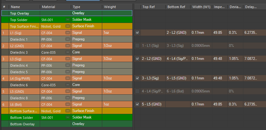
When the trace length exceeds the critical length, controlling the impedance becomes essential. Adjusting the trace width based on the chosen stackup and build-up ensures a specific transmission line impedance. Altium Designer offers a robust 2D field solver to calculate required trace widths quickly.
Tip #4: Trace Length and Spacing
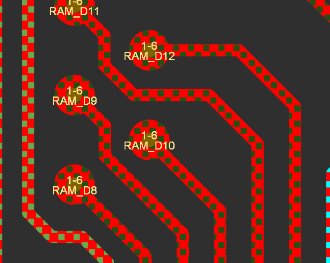
Keep high-speed traces as short as possible to minimize EMI and SI. Maintain a distance between different high-speed traces to reduce crosstalk. Aim to keep high-speed traces away from components like inductors or power sections, following the “3 h rule” where traces should be separated by at least three times the height of the dielectric between the signal layer and the next ground or reference layer.
For top-notch, high-speed designs, simulation tools become essential to verify compliance with required signal integrity and EMI standards.
Correo electrónico: altium@americarep.com
Mexico +52-33-2736-0777
Argentina +54-911-5381-8404
Chile +54-911-5381-8404
USA +1-915-777-3078
Altium Designer 24 está disponible ahora .
Leave a Reply